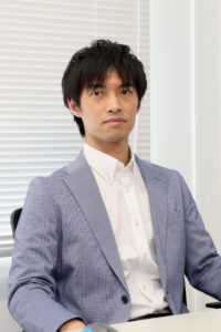
Member
Fumihiro INOUE
 |
Affiliation
Yokohama National University, Graduate School of Engineering Science, Department of Systems Integration Career History
|
Linkedin: https://www.linkedin.com/in/fumihiro-inoue-15a75595/
Google Scholar: https://scholar.google.co.jp/citations?user=NChzX-cAAAAJ&hl=ja
ORCID: https://orcid.org/0000-0003-2292-846X
YNU: https://er-web.ynu.ac.jp/html/INOUE_Fumihiro/en.html
Research Laboratory Members (Fiscal Year 2025)
Senior Specially Appointed Prof.
Kazuyoshi Ueno
Associate Prof.
Taku Yanase
Assistant Prof.
Marie Sano
Assistant Prof. (IMS Specially Appointed Assistant Professor)
Nyamjargal Ochirkhuyag (Nima)
D Y. N
D L. M
D K. N
D A. F
M2 H. K
M2 Y. M
M2 R. S
M2 K. H
M2 Y. Y
M2 D. K
M1 Y. K
M1 Y. O
M1 R. O
M1 T. Y
M1 F. T
M1 S. U
B4 H. I
B4 S. M
B4 T. M
B4 S. M
B4 R. K
Lab Assistant (Technician)
A. O
S. A
Lab Assistant (Office work)
K. Y
S. N
C. Y
S. H
Project Assistant
S. S
N. M
Manager
H. K
Offices and Laboratories
Mechanical Engineering and Materials Science Building → Office, Mechanical Laboratory
Chemistry Building → Chemical Laboratory
Integrated Research Building → Semiconductor Measurement and Evaluation Laboratory, Office
Faculty of Education, Research Building No.3 → Office of the Semiconductor and Quantum Integrated Electronics Research Center, Semiconductor Process Laboratory
For those considering joining our laboratory (undergraduate 4th year students, international students and those who are considering applying for graduate school)
Our research target is 3D integration technology, which is essential for the next generation of semiconductors. We have already initiated several large-scale collaborative research projects and national projects and have introduced state-of-the-art equipment and the only measurement devices in the world.
The field of semiconductors does not mean just electrical/electronic engineering. We study mechanical engineering related to semiconductor manufacturing. You should be able to apply what you have learned in your classes so far.
- You may have found the research introduction to be very difficult to understand, or perhaps you misunderstood and thought you could make CPUs or memory modules yourself.
- However, actual university research tends to be quite simple (even research in companies and research institutes often involves simple tasks and repetitive work).
- Only part of the process can be researched at the university. We aim for practical application through collaborative research with companies.
- You don’t need to understand everything as an undergraduate student.
- In fact, it is natural to repeat the same experiments with different conditions and materials in actual research projects. However, we aim to clarify principles and deepen understanding by adding new materials and special conditions.
Rarely, new discoveries or phenomena may be found in the process. Although, you will develop an attitude of conducting research and analysis by repeating such processes and practicing basic research, such as looking through relevant technical literature and English papers.
People suitable for our laboratory
- Those interested in the semiconductor field or industry, or those whose desired future field is undecided. (The perception that Japanese semiconductor industry is declining is incorrect! Equipment and material vendors are still active worldwide. Semiconductors are not disappearing. Rather, they are a growing field that will become even more necessary).
- Individuals interested in applying to graduate school in the future and participating in overseas conference presentations or internships abroad (research exchange programs).
- Those with a pioneering spirit, vitality to research anything on their own, and a willingness to take on challenges.
We welcome the participation of students who possess an interdisciplinary (cross-border) perspective, a desire to advance into new fields, a rich spirit of inquiry for nurturing scientists and engineers, and a strong spirit of challenge.
