Research Content
3D Integration/Chiplet
In advanced semiconductors, achieving high integration and low power consumption based on the miniaturization rule (Moore’s Law), which has been considered a key indicator, poses challenges in terms of development, investment costs and design optimization.
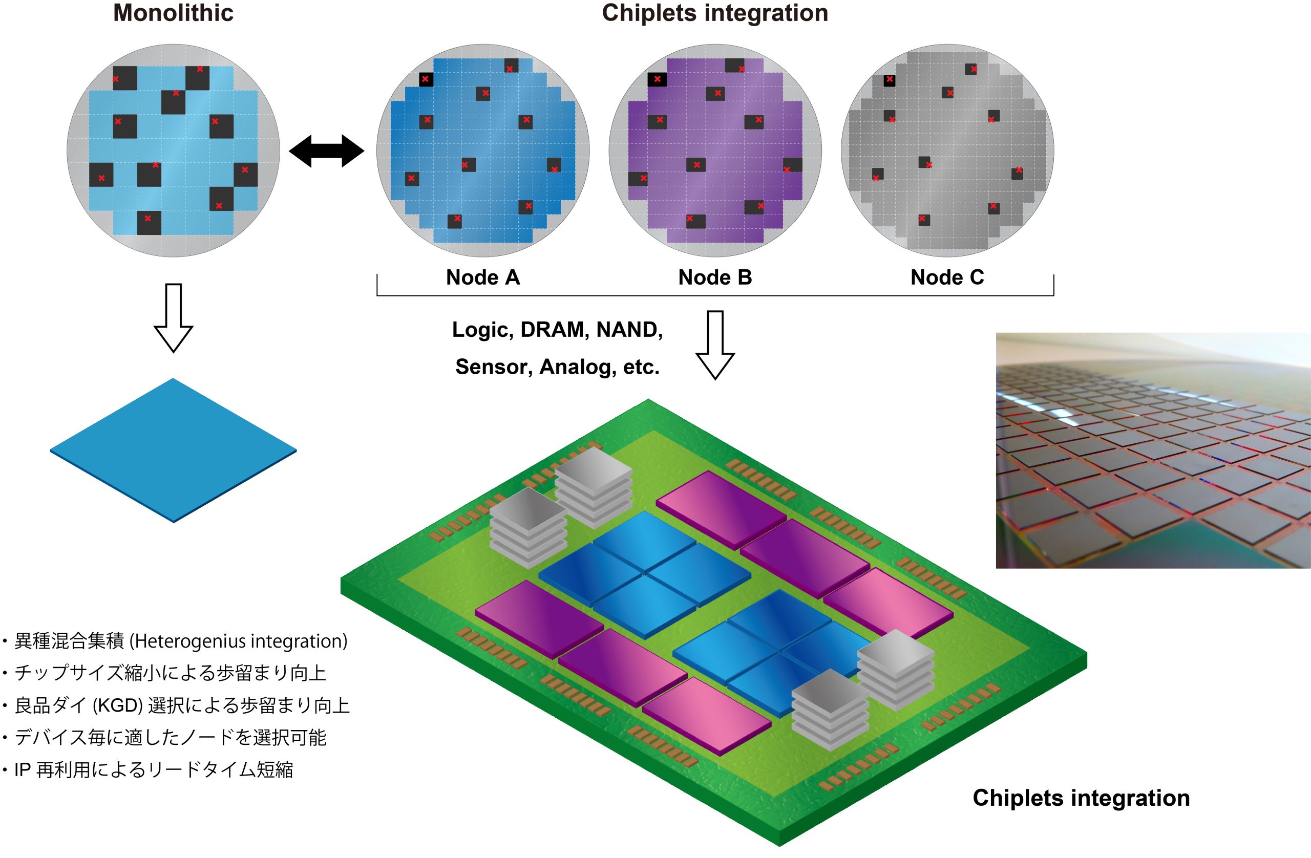
To overcome these challenges, the design philosophy and integration technology of “chiplets” have emerged. Chiplets involve dividing the required functions, manufacturing them at appropriate technology nodes with high yield, and connecting and packaging them using semiconductor post-processing assembly techniques. This enables high integration, shortening of Time to Market, and optimization of wiring for low power consumption.
The basic concept of chiplets is not to integrate all elements on one side of the die (chip) (i.e., monolithic), but to create various components along the required technology nodes and then assemble them later, connecting them on the substrate through wiring.
To achieve low power consumption through miniaturization with monolithic designs, many processes must be repeated, and defects increase as the die area increases. On the other hand, chiplets not only enable good selection but also allow for wiring redesign and optimization, leading to very high energy efficiency. Furthermore, it is believed that productivity and yield can be improved by creating smaller chiplets and “connecting” them.
While chiplets themselves may not represent a technological breakthrough, without this design/manufacturing concept, it is becoming increasingly impossible to economically manufacture low power consumption semiconductors that meet the demands of various applications.
3D heterogeneous devices
Looking further into 2050, electronic devices play a crucial role in all of these areas: the automation of transportation equipment through technologies like autonomous driving, the development of smart cities through Beyond 5G technology, digital services enabled by VR/AR, and remote medical care through online diagnosis. Achieving such advanced final applications cannot be accomplished solely through miniaturization and high integration or performance of individual devices. Instead, it requires “heterogeneous devices” capable of highly parallel operation of various devices such as memory, logic, power devices, various sensors, and optical devices.
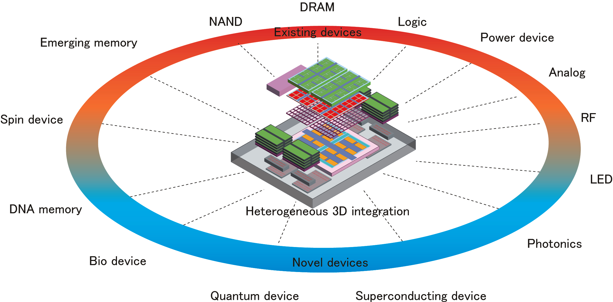
In this research laboratory, we focus on researching “back-end process technology” for 3D heterogeneous device.
Main Research Themes
1.Hybrid bonding
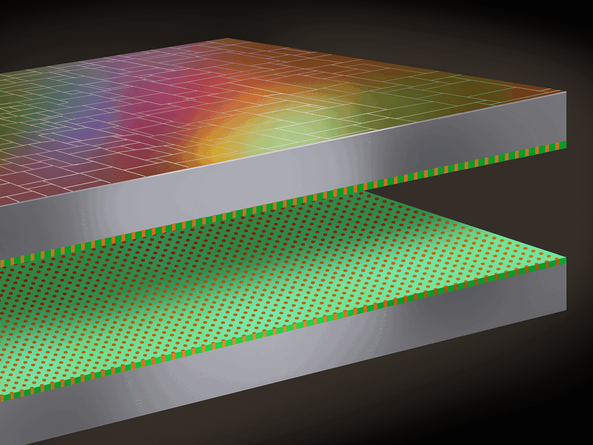
In wafer-to-wafer bonding technology for stacking heterogeneous devices on wafers, which has evolved from direct bonding and connection via Via-last TSV, there is currently intense competition in the development of “Cu-SiCN hybrid bonding,” which offers greater design flexibility. This technique involves bonding surfaces formed by damascene processes through plasma surface activation, achieving both mechanical bonding of insulating films and electrical bonding of metals in a single bonding step. Additionally, for chiplets and 3D heterogeneous devices, the development of Die-to-Wafer (D2W) bonding technology is crucial, allowing die size variability and die selection (KGD). Conventional D2W bonding uses thermal compression bonding utilizing the eutectic reaction of tin (solder), but this method faces limitations in reliability and alignment accuracy at narrow pitches. Research and development competition is ongoing for breakthroughs in bonding pitch reduction using “hybrid bonding”.
Our research laboratory is one of the few in the world advancing research in all aspects of plating, CMP, and direct bonding for hybrid bonding. Furthermore, we also conduct research on pre-assembly techniques (dicing, die-level cleaning, etc.).
2.Chemical Mechanical Polishing (CMP)
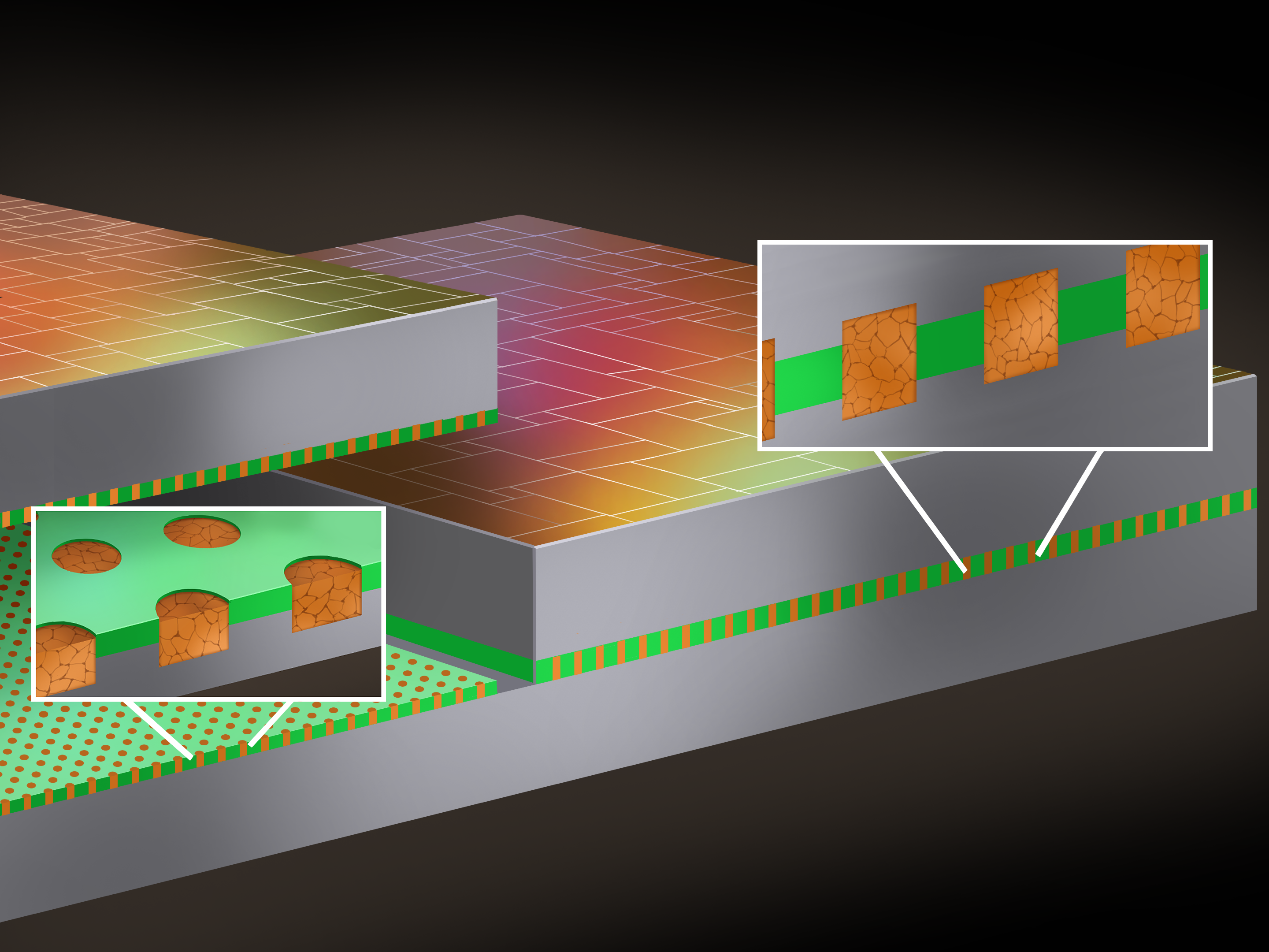
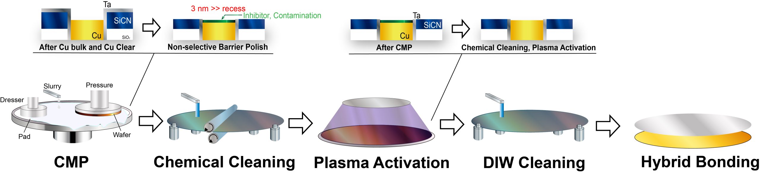
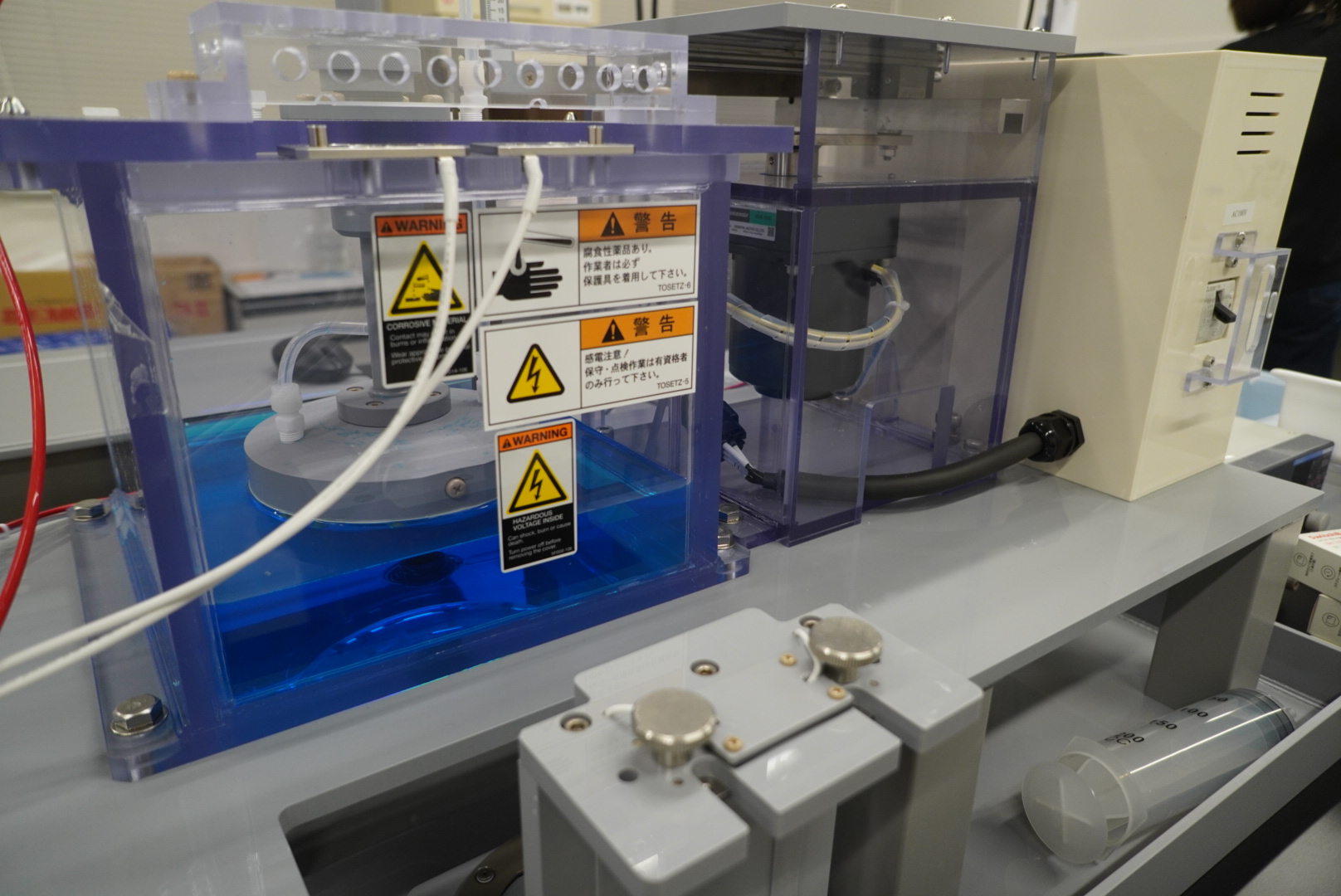
The accuracy of hybrid bonding greatly depends on the finish of the wafer surfaces being bonded. Therefore, chemical mechanical polishing (CMP), which plays the role of surface finishing, is crucial. CMP equipment works by using abrasive grains suspended in a slurry, which, along with the chemical action of the slurry and the physical action of the polishing pad, polish the wafer.
The CMP process for hybrid bonding is mainly divided into three steps: Cu polishing, Cu removal, and Ta removal and planarization. Currently, the challenge lies in the third step, Ta removal and planarization. Planarization here refers to flattening the Cu, Ta, and SiCN films. If not properly adjusted, Cu, being more electrochemically active than Ta, will corrode more easily than Ta, leading to recesses. Conversely, if corrosion is too suppressed, Cu protrusions may occur. To address this challenge, it is necessary to minimize the polishing selectivity between Cu, Ta, and SiCN.
Additionally, it is crucial to suppress recesses in post-CMP cleaning and surface activation before bonding.
To achieve these goals, we are conducting evaluations through electrochemical measurements, zeta potential measurements, cleaning, plasma activation, and actual polishing.
Furthermore, in the future, we plan to challenge not only hybrid bonding but also polishing in post-Cu materials for fine wiring.
3.Cu Plating
In hybrid bonding, the crystallinity and grain size of Cu are also crucial. These factors are determined by the plating process. We are plating Cu films suitable for hybrid bonding, called “Designer Cu”, using novel additives.
4.Bonding Strength Measurement
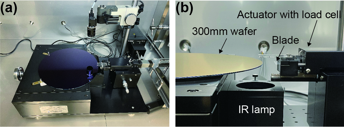
Furthermore, in addition to integration technology and component technology, we are advancing the development of essential techniques from a unique perspective, which is globally required, in “measurement and evaluation methods” for new chiplets. We are particularly focused on the bonding strength measurement methods in hybrid bonding. In wafer-to-wafer (W2W) hybrid bonding, a method called the Double-Cantilever Beam (DCB) is used to measure bonding strength by inserting a razor blade. Regarding this method, our laboratory is conducting research towards manual international standardization.
Additionally, bonding strength at the die level is an essential evaluation item in device development such as bonders and dicing, and we are putting effort to create a method using nanoindentation as a new evaluation technique.
5.3D Quantum Computer Integration Technology
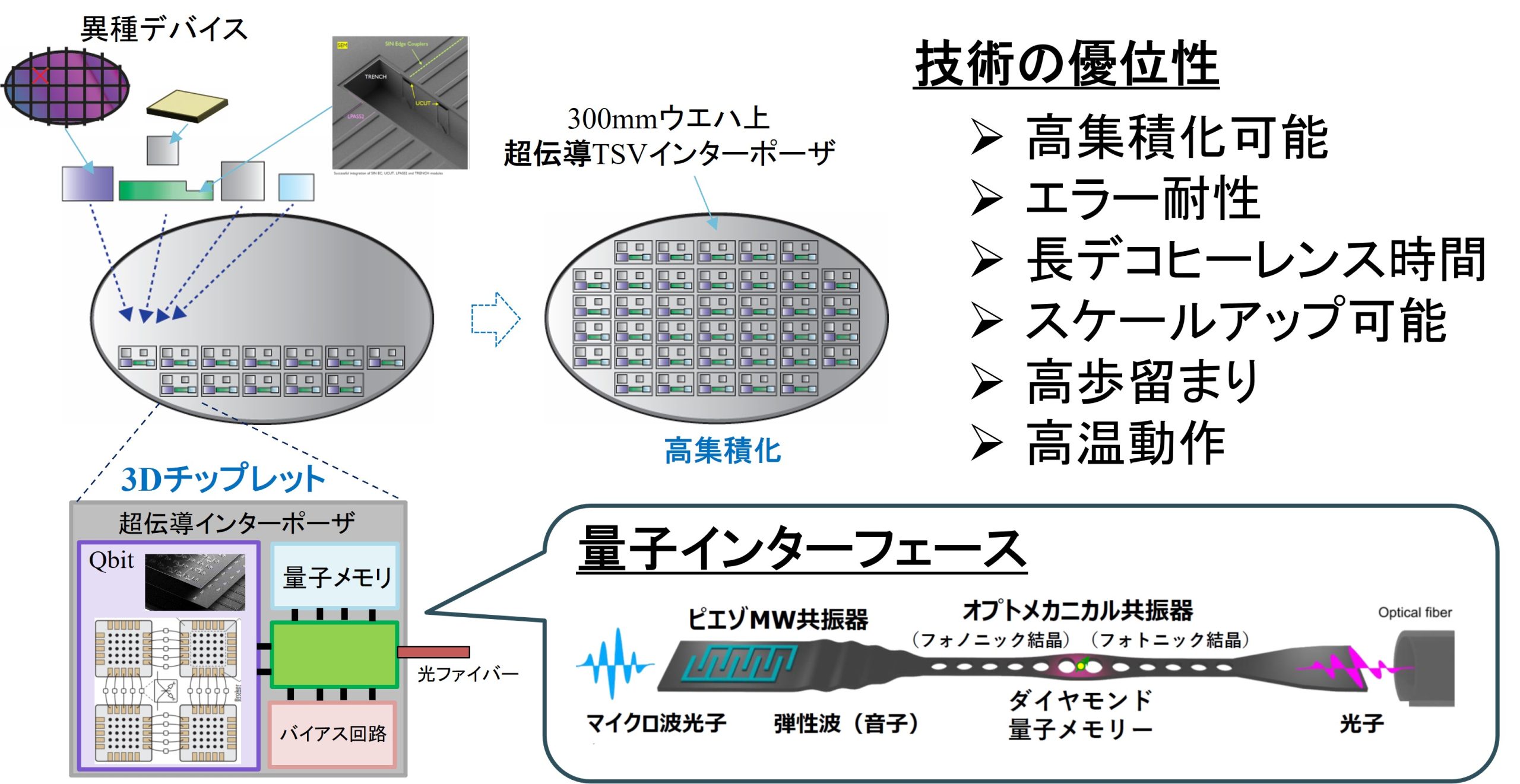
In quantum computer, the number of Qbits determines the calculation speed of quantum operations, and as this number increases, the calculation speed increases exponentially. For the future scaling up of quantum bits, it is essential to integrate control circuits with Qbits. Since quantum bits and control circuits use different types of superconducting integrated circuit technology, “heterogeneous device integration technology” is required. Additionally, for error correction of quantum bits, surface codes, for example, are used, but for this, 3D stacking with microwave circuits is essential. The three-dimensional quantum computer (3D-QC), which creates quantum bits, other computational circuits, and superconducting elements separately and connects them using three-dimensional implementation technology, is highly anticipated.
In our research laboratory, we study superconducting TSVs, superconducting hybrid bonding, and other technologies, aiming to realize this 3D-QC.